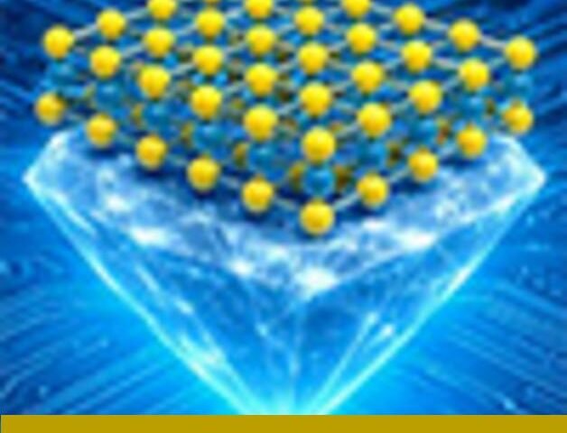
Placing an atomically thin layer of molybdenum disulfide (MoS2) onto a diamond substrate produces measurable current flow at room temperature, a material combination that opens a practical pathway for diamond‑based electronic circuits. The demonstration removes a key thermal and interface barrier that has limited diamond’s use in conventional electronic architectures and signals a new integration approach for high‑performance devices.
- Material: molybdenum disulfide (MoS2) layered on diamond
- Key result: sustained current flow at room temperature
- Technique: stacked 2D materials forming a van der Waals interface
- Device implication: enables diamond‑based electronic circuit pathways
Context: how this fits current materials and device trends
The result sits at the intersection of two 2025–26 trends: the rise of 2D semiconductors as complementary channels and renewed interest in diamond as a wide‑bandgap, thermally conductive substrate. MoS2 brings an atomically thin, direct‑gap semiconductor layer whose carrier transport characteristics can be tuned by interface engineering. Diamond contributes substantial thermal conductivity and a robust lattice that, when paired with a van der Waals‑bonded 2D film, can support electronic functionality without the cooling overhead that has previously constrained experimental devices.
For designers and materials engineers the tactile realities matter: atomically flat MoS2 provides a uniform conduction plane while the diamond interface mitigates hot‑spot formation through high thermal diffusivity. The stacking approach — layering ultrathin films to form clean, low‑defect interfaces — is consistent with foundry workflows for heterogeneous integration, making the result technically accessible to companies exploring next‑generation RF, power or sensor platforms.
Impact: why US manufacturers, investors and suppliers should take note
For US device makers and foundries, room‑temperature conduction across a MoS2–diamond interface reduces a key barrier to productisation. Removing the need for cryogenic or exotic cooling strategies lowers system complexity and cost, changing how engineers size thermal management and select substrates. That shift has implications for bill‑of‑materials, manufacturing yields and margin structures for high‑performance modules.
Suppliers of synthetic diamond substrates and 2D material producers could see new demand vectors from companies building RF amplifiers, power switches or compact sensors that prioritise thermal performance and reliability. For investors, the result signals an early commercialisation pathway: integration‑focused startups and established materials firms that can scale wafer‑level bonding or transfer processes will be strategically advantaged.
In market messaging and specification sheets, manufacturers should emphasise measurable device attributes — carrier transport at operational temperature, interface defect density and thermal conductance — rather than aspirational claims. Standards around characterization and repeatable stacking will be the practical next step to convert this materials advance into deployable, revenue‑generating products in the US electronics ecosystem.
Image Referance: https://www.nanowerk.com/nanotechnology-news3/newsid=68521.php